Emilie's PhD Research
Welcome to this blog post! I’d like to tell you a bit more about my PhD work and journey.
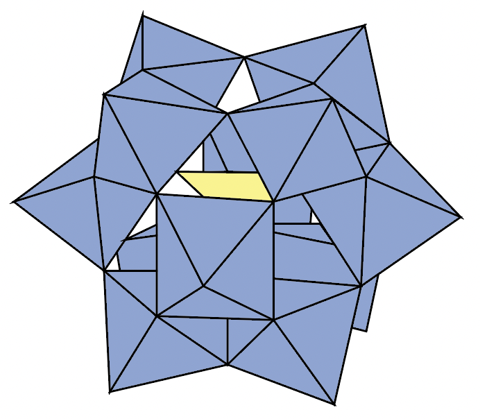
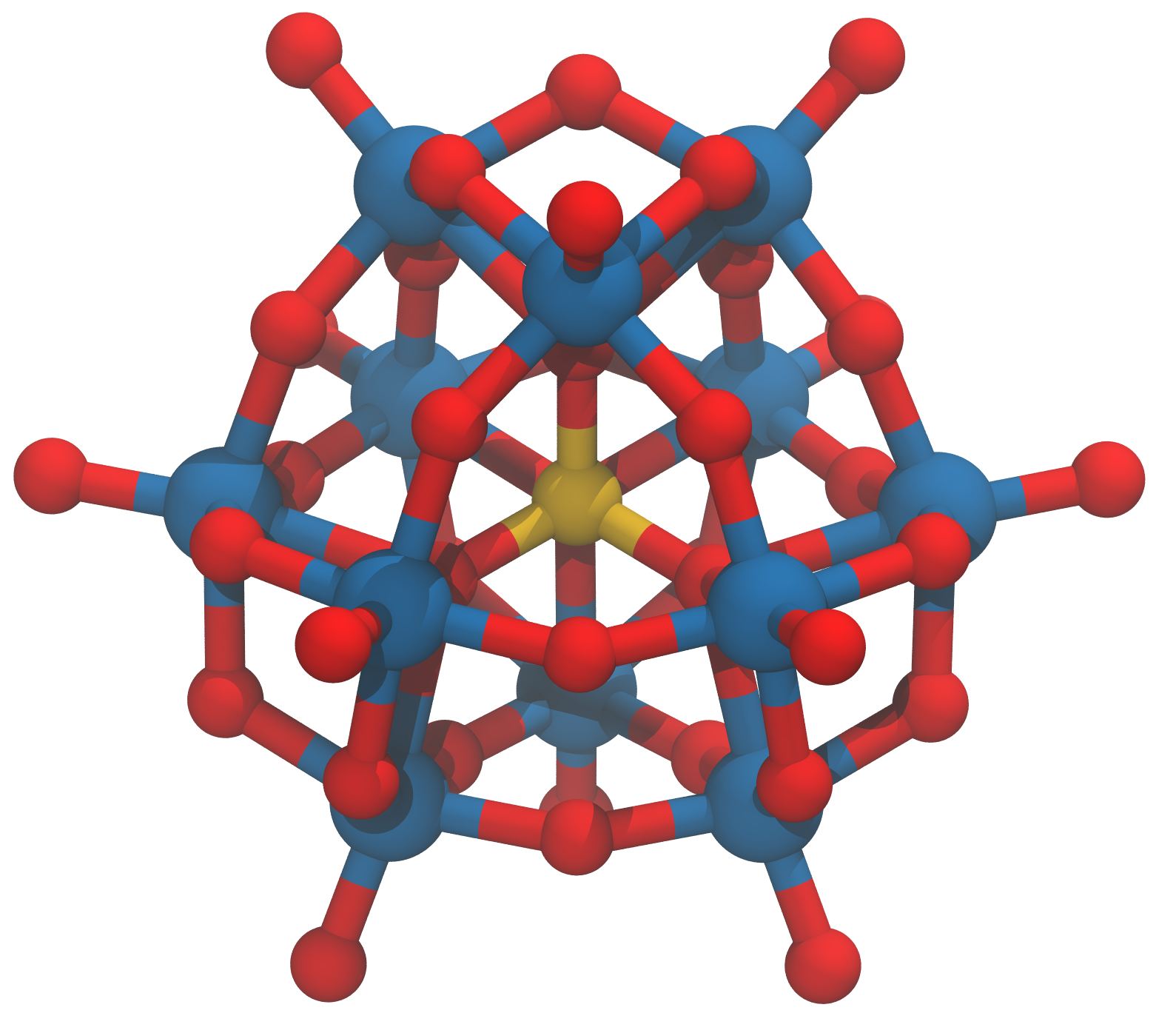
During my PhD, I studied how I could use polyoxometalates (or POMs for short - see the pictures below) to make better electronic memories.


If reading isn’t quite your thing, you could have a look at this short video I made explaining my work!
The issue with the current electronic memories we have is that they’re reaching their limits. We are continuously asking for faster, smaller, and more energy-efficient devices. Therefore, we need new types of electronics, and electronic memory devices. An example of an up and coming technology is the resistive random access memories (or RRAM for short). The main difference with the traditional transistor technology is that it only needs two electrodes, instead of the three. So, to make these RRAM devices, you simply sandwich a material of choice between two metal electrodes. In my case, I studied POMs as my material choice.
Now, let me tell you more about POMs and why they’re great to make electronic memories. They are metal oxide nanoparticles, which means that they are made of metal and oxygen atoms, and are roughly 1 nm in size. Here are a few of their amazing properties:
- they can withstand a wide temperature range (-195 to 400 °C)
- they are soluble in many solvents even non-toxic and water based ones, which makes them very easy to process
- their structure is very easy to modify, and different chemical groups can be added to their base structure, therefore, it’s possible to tailor POMs properties to specific applications
- finally, most importantly, they can reversibly exchange multiple electrons with little structural change, meaning that different memory states can be stored via different number of electrons
The last sentence is a bit tricky to understand, but very important. The help explain it better, we need to use electrochemistry. When I say “POMs can reversibly exchange multiple electrons”, I mean that they have many redox states. And therefore, the different redox states of the POM are the different states of the memory device. The traditional transistors have two states: “on” and “off” or “1” and “0”. But with POMs, we could have many more states. This is very useful because it means that we can store more information in a single device, which is exactly what we want to make more efficient devices. Devices using this concept of storing multiple states in a single device using the material’s redox states are called redox-based resistive random access memories (or ReRAM for short).
After talking about the material choice, the last point I’d like to discuss in this section, is the electrode choice. RRAM devices only need two electrodes, which can be arranged in different ways as shown in the image below. They can be either vertical (also called sandwich) or coplanar.

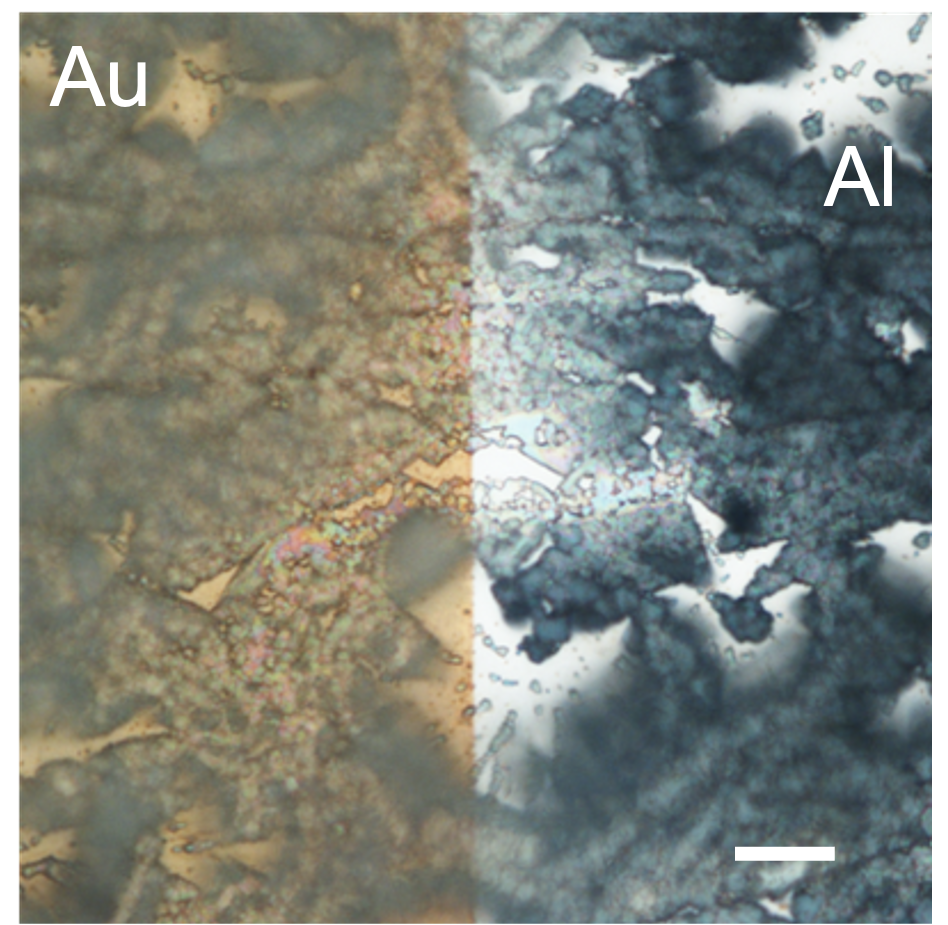
Since I’m working with POM nanoparticles, the best configuration is “coplanar”. Because POMs don’t form very continuous films: there are some pinholes in the film (see image below). The issue with these pinholes is that in a vertical architecture, the top electrode could penetrate the film and directly come into contact with the bottom electrode and shorting the device. Therefore, the coplanar configuration is the best choice for POMs. To even more optimize the device layout, the two electrodes could be coplanar, but separated by a nanogap. This would help the device to be faster and more energy-efficient.

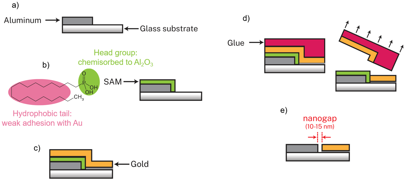
However, fabricating nanogap separated coplanar electrodes can be quite expensive! For example, e-beam lithography is very precise, but is also very expensive. Therefore, I used a technique called “adhesion-lithography” to make my electrodes. It is compatible with large area substrates, can produce many devices quickly and efficiently, and is low-cost. The steps are shown in the image below.
To start, the first electrode is deposited on the substrate and patterned via standard photolithography. In my case, I chose to work with aluminium (Al for short). Next, the entire substrate is dipped in a carefully chosen self-assembled monolayer (or SAM for short) molecule solution. This SAM choice is important as it must attach only to the first electrode and not the substrate. Therefore, in this case, since I work with an aluminium electrode and glass substrate, I chose octadecylphosphonic acid (ODPA for short). The ODPA molecule has a phosphonic acid head group (green in the image) that attaches to the Al electrode and a long hydrophobic tail (pink in image), which will be important later. The next step is to deposit the second electrode all over the substrate without any patterning. In my case, I use gold (or Au for short). Then, a glue is applied to the entire substrate, left to dry, and peeled off. Now is when that SAM’s hydrophobic tail is important. Since it’s only on the aluminium electrode, the gold on top of it isn’t strongly attached and can be peeled off. However, the gold on the glass substrate is strongly attached and remains on the substrate: there was no SAM in the way. The last step is to remove the SAM in order to get the nanogap separated coplanar electrodes. This can be done by simply ozone ashing the substrate, which will burn away the organic SAM molecules.

This technique is compatible with different device architectures. The two electrodes can have many designs. In my work, I was simply interested in studying this combination of POM with Al and Au electrodes, so I used simple square patterned devices (see below). The first three images are a top view of the finished electrodes. The last image is a cut view of the electrodes to better show the nanogap.
The first image shows that 81 devices can be comfortably fit on a 2x2 cm glass substrate. Each gold square is one memory device. The second image shows a zoomed-in view of a single device: each side measures 1 mm. The third image shows an even more zoomed-in view of the interface between the Al and Au electrodes: the nanogap is quite smooth and uniform. Finally, the last image is a cut view of the electrodes to better show the nanogap, which itself measured about 20 nm.

And there we have it! The electrodes are made, now we simply need to deposit the POMs in the nanogap, and get testing the device! I’m currently waiting on my research paper to get published, then I’ll make a new blog post about the results. So stay tuned!
Here are some references you can check out if you want to learn more:
- Electronic memory technologies: Semiconductor Memories and Systmes; Redaelli, A., Pellizzer, F., Eds.; WoodHead Publishing Series In Electronic and Optical Materials; Woodhead Publishing: Cambridge, MA, 2022.
- Polyoxometalates: Pope, M. T. Heteropoly and Isopoly Oxometalates; Jørgensen, C. K., Lappert, M. F., Lippard, S. J., Margrave, J. L., Niedenzu, K., Nöth, H., Parry, R. W., Yamatera, H., Series Eds.; Inorganic Chemistry Concepts; Springer Berlin Heidelberg: Berlin, Heidelberg, 1983; Vol. 8.
- Adhesion-lithography: Semple, J.; Georgiadou, D. G.; Wyatt-Moon, G.; Yoon, M.; Seitkhan, A.; Yengel, E.; Rossbauer, S.; Bottacchi, F.; McLachlan, M. A.; Bradley, D. D. C.; Anthopoulos, T. D. Large-Area Plastic Nanogap Electronics Enabled by Adhesion Lithography. npj Flex Electron 2018, 2 (1), 18. https://doi.org/10.1038/s41528-018-0031-3.
Enjoy Reading This Article?
Here are some more articles you might like to read next: